


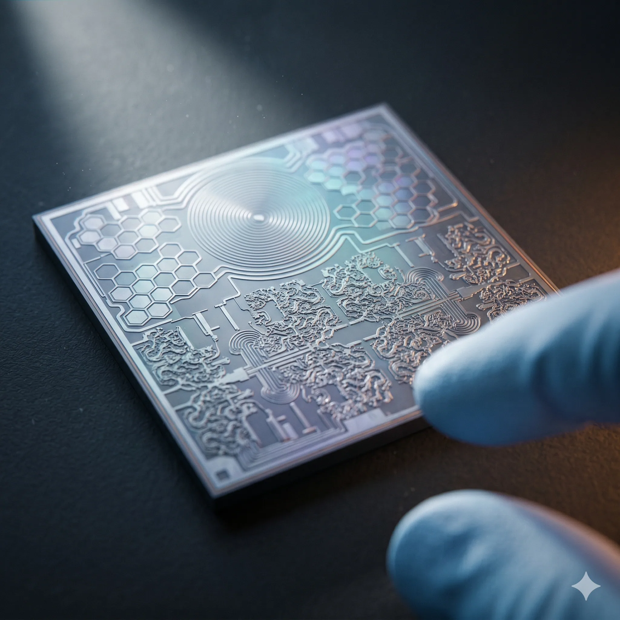

G1 Layout
Floor-plans organised around the locality patterns the substrate already prefers.
Blocks that talk to each other sit next to each other. The wire length budget is paid where it matters; the rest pays nothing.
One architecture on a continuous axis — reared on the stack.
Explore LoominumEnterprise
Research
Science
About
Silicon where physics already does some of the work.
Silicon where the physics and the geometry of cognition are designed together.
Compute is geometry: how charge moves, how signals route, how locality is enforced. Most chips treat that geometry as constraint. We treat it as substrate. Geometry-native compute means designing silicon whose layout, analog blocks, and signal paths share the primitives our cognitive substrate uses, so the physics is already doing some of the work.
Floor-plans organised around the locality patterns the substrate already prefers.
Blocks that talk to each other sit next to each other. The wire length budget is paid where it matters; the rest pays nothing.
References and sense paths designed against the cognitive primitives, not the other way around.
Bandgap, PTAT, and the sense path are tuned to the substrate, not retrofitted to it. The reference is part of the model, not a tolerance.
Root-of-trust, sealed storage, and post-quantum signing live inside the same fabric as compute.
TPM + secure memory + sealed storage + BCH + Shamir + audit log + lockout + wallet-backed ML-DSA signing — drop-in surface, not bolt-on.
Numbers below are measured from the GDS, not from a planning slide. They are the only scoreboard a tape-out has.
A drop-in bundle, not a bolt-on. Ten components shipped together, with a wallet-backed post-quantum signing surface and an analog NTT study at the bottom.
A functional substrate for adaptive compute with the full developmental stack on top.
Bandgap IP closed; PTAT verified in SPICE; sense-amp and PTAT layout in active iteration.
TPM, secure memory, sealed storage, BCH, Shamir, audit log, lockout, and a wallet-backed post-quantum signing surface, with an RTL skeleton and an analog NTT study.
Phase-6.A2 control top-level block closed on a foundry process. 101k cells, zero DRC, LVS clean.
The differentiating bet is that the substrate and the silicon should share an organising principle. Where they do, the system gets locality and energy for free, because the physics is already doing the work the abstraction would otherwise have to enforce.